PRESENTATION
Advancing Scalable Photonic Integration: Heterogeneous Integration of Active Components for Next-Generation Applications
This presentation explores how heterogeneous integration is revolutionizing photonic integrated circuits (PICs) by combining diverse materials with active components. We demonstrate advances in wafer-scale integration, enabling high-speed modulators and photodetectors on low-loss passive platforms for applications in space communication, quantum technologies, LIDAR, and biosensors.
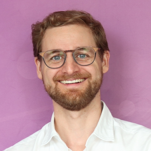
Michael Geiselmann
LIGENTEC
Michael Geiselmann is Co-Founder and CCO of LIGENTEC SA, a photonics company with headquarters in Switzerland, production in France, and an office in Belgium. He earned his PhD at ICFO, Barcelona, and advanced frequency comb research at EPFL. In 2016, he co-founded LIGENTEC, bringing cutting-edge photonic integration to the global stage.

