17th edition / co-located with AngelTech
Connecting the compound semiconductor community.
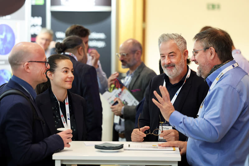
CS International 2027 is the flagship annual gathering for the compound semiconductor industry, bringing together the full supply chain for three days of technical talks, networking and an exhibition floor.
- 750+Attendees
- 80+Exhibitors
- 30+Presentations
About CS International
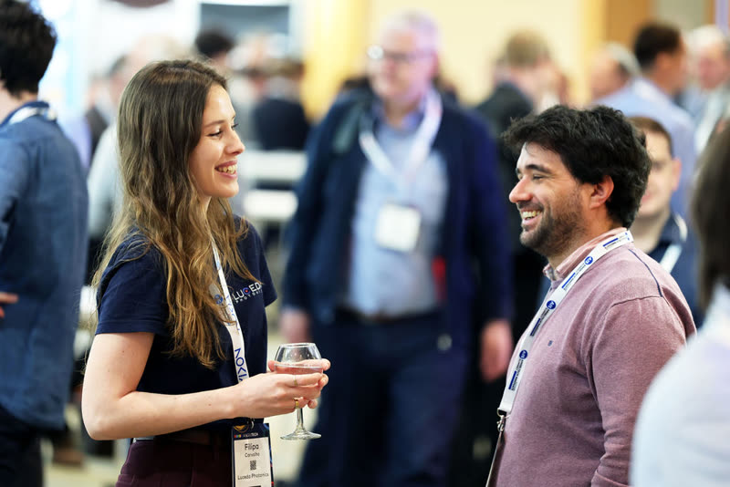
Connecting the CS Industry
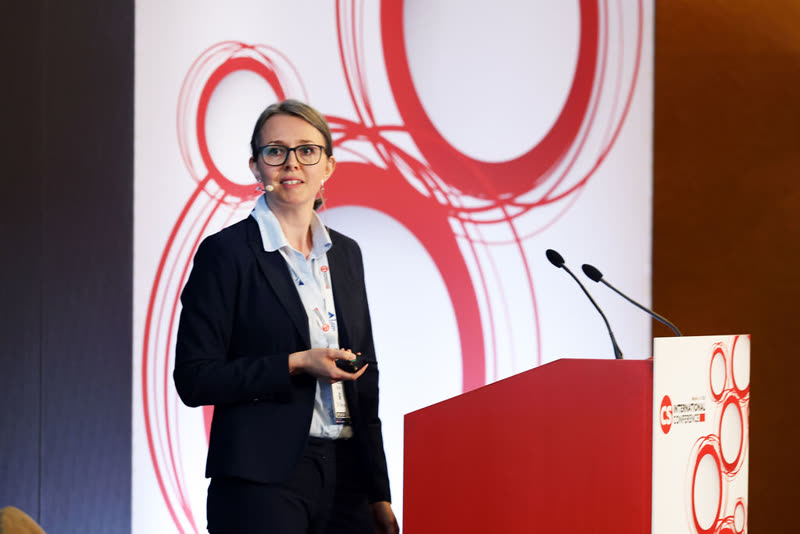
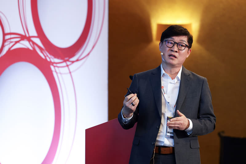
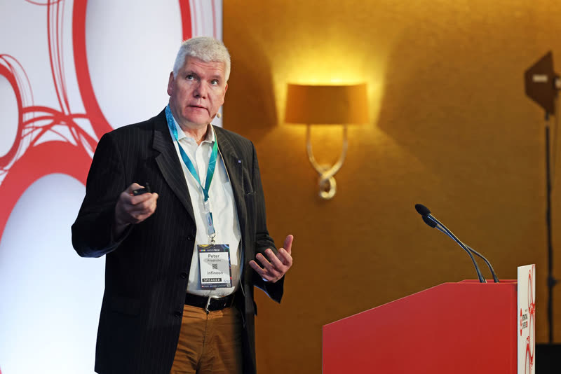
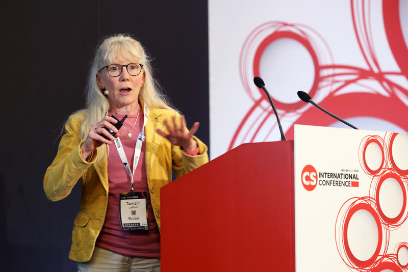
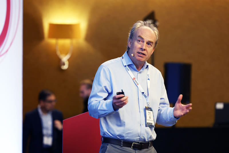
The 17th CS International builds on the huge success of the 2026 event and the strengths of its predecessors, with around 40 leaders from industry and academia delivering presentations across four key themes:
- AI: Who will be the biggest winners?
- Gaining an edge in the power industry: scale and strategy
- Strategies in photonics: Identifying the best opportunities
- Making money from trailblazing tech
Delegates attending these sessions will gain greater insight into device technologies while learning about the latest opportunities and trends within the compound semiconductor industry. Those attending CS International will also hear about significant advances in tools and processes that deliver enhanced yield and throughput.
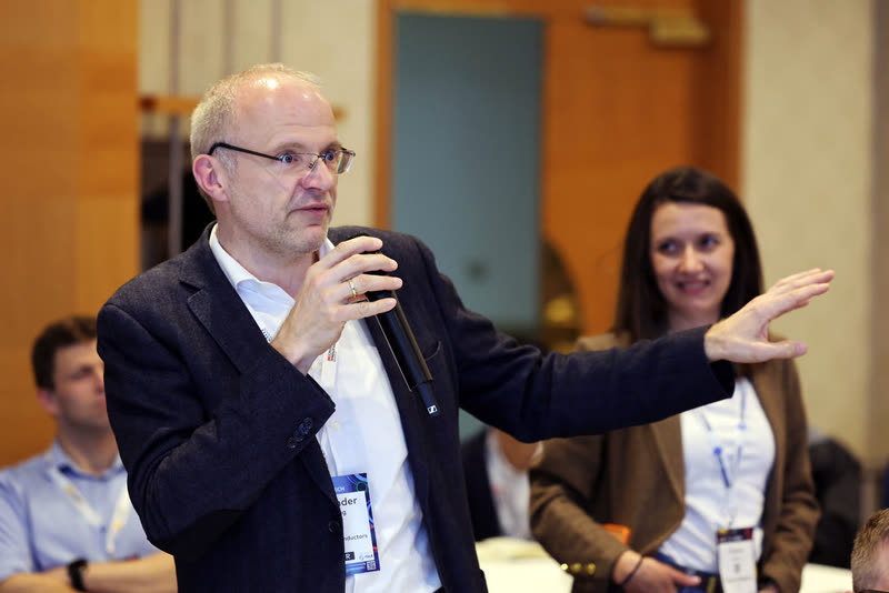
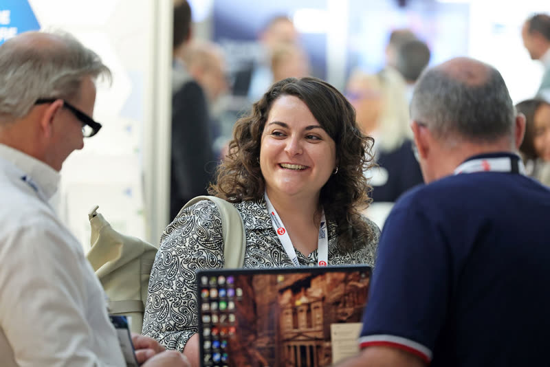
Attendees at this two-day conference will meet a wide variety of key players within the community, from investors and analysts to fab engineers and managers.
CS International is part of AngelTech, bringing together an Innovation Summit, four co-located conferences and an exhibition with more than 120 presentations, more than 850 attendees and over 80 exhibitors. AngelTech is the only global event covering Compound Semiconductor, PICs, Power Electronics and Advanced Packaging technologies, bringing key executives together under one roof for three days of networking and insight.
Register for 2027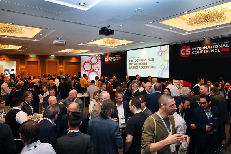
2027 Speakers
CS International 2027 speakers include
Sponsors & Exhibitors