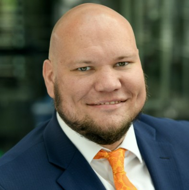
Andreas Fiedler
Group leader: Aluminum-Gallium-Oxide-Electronics (All-GO-HEMT NanoMatFutur project funded by BMBF)
Leibniz-Institut für Kristallzüchtung (IKZ)
Andreas Fiedler is the head of the research group for transport and electrical properties at Leibniz-Institut für Kristallzüchtung (IKZ, Leibniz-Institut für Kristallzüchtung) in Berlin. He studied physics at Humboldt-Universität zu Berlin, focusing on electrical characterization of thin films while earning his master’s degree in 2013. In 2015, Fiedler started working on his doctoral degree at IKZ, with focus on the characterization of single crystalline β-Ga2O3 in form of bulk crystals grown by Czochralski method as well as in form of layers grown by MOVPE. He was recognized for his outstanding achievements in the field by The Ohio State University's (OSU) 2019 Presidential Postdoctoral Scholars Program. During his postdoctoral studies at OSU he increased his portfolio skills by working on the processing and characterization of power electronics based on β-Ga2O3. In March 2022 he returned to IKZ, where he fulfills now a key position for material characterization as group leader. At the beginning of 2025, Andreas Fiedler was selected as one of the few outstanding young scientists in the prestigious NanoMatFutur program funded by the Federal Ministry of Research, Technology and Space (BMFTR) of Germany.
Presentations
Towards More Efficient Power Transistors: Modulation-Doped β-(AlₓGa₁₋ₓ)₂O₃/Ga₂O₃ Heterostructures with Enhanced Electron Mobility
Semiconductor-based power electronics is a key technology for solving the greatest challenge facing society - sustainable energy generation. This challenge is to be tackled by developing modulation-doped β-(AlxGa1-x)2O3/Ga2O3 heterostructures with high electron mobility for highly efficient power transistors. In Ga2O3 in particular, this approach to increase the charge carrier mobility promises a high innovation potential, as it was also theoretically predicted that the significantly limiting scattering process on polar-optical phonons would be screened. If this scattering process is suppressed, a similar charge carrier mobility is expected in Ga2O3 as in silicon, as the effective electron mass is similar. Effective screening of polar-optical phonons only occurs at a carrier density in the two-dimensional electron gas (2DEG) around 1013 cm-2, which requires a conduction band discontinuity of at least 1 eV. Theoretical predictions show that this requires an aluminum content of at least 50% (x ≥ 0.5) in the barrier. This structure has not yet been realized and is to be developed for the first time in the All-GO-HEMT project. The requirements for high crystalline perfection, a homogeneous layer thickness and smooth interface with a high Al content and delta doping over the entire substrate size of up to 2 inches must be met to provide a material basis for more efficient power electronics.

