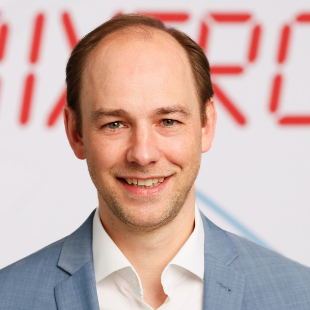
Dr. Nicolas Muesgens
Director Product Manager GaN
Aixtron
Dr. Nicolas Muesgens holds a PhD in Physics from RWTH Aachen University in Aachen, Germany. With nearly 15 years at AIXTRON, he has held various roles in Technology, Project Management, Service, and Product Marketing. Currently, he is responsible for AIXTRON’s GaN-based High Volume Manufacturing (HVM) products, overseeing the assessment of the GaN market for Power & RF and MicroLED applications. Dr. Muesgens also defines AIXTRON’s GaN Epitaxy HVM product roadmap, covering wafer sizes from 100 mm to 300 mm. With around 15 years of experience in MOCVD technology across Germany and Asia, he is a seasoned expert in the field.
Presentations
Leading Epitaxy Solutions for High Volume Manufacturing of Compound Semiconductor & Optoelectronic Devices
The rapid expansion of artificial intelligence (AI) infrastructure is reshaping global semiconductor demand. AI-driven data centers require highly efficient power conversion and ultra-fast optical interconnects, accelerating the adoption of SiC and GaN for power electronics, as well as InP- and GaN-based materials for lasers and micro-LEDs used in optical communication. Transitioning these technologies to high-volume manufacturing requires industry-leading epitaxial uniformity, reproducibility, and cost efficiency on wafer sizes scaling from 150 mm up to 300 mm. Increasing wafer diameters place additional demands on thermal management, process stability, and yield control. This contribution highlights how our products address these requirements by enabling high throughput and high epitaxial yields for the growth of SiC, GaN, as well as InP- and AsP-based materials. By combining advanced reactor design with optimized process control, we enable reliable, scalable, and cost-effective high-volume production of compound semiconductor devices powering the AI-driven era.

